


Overview
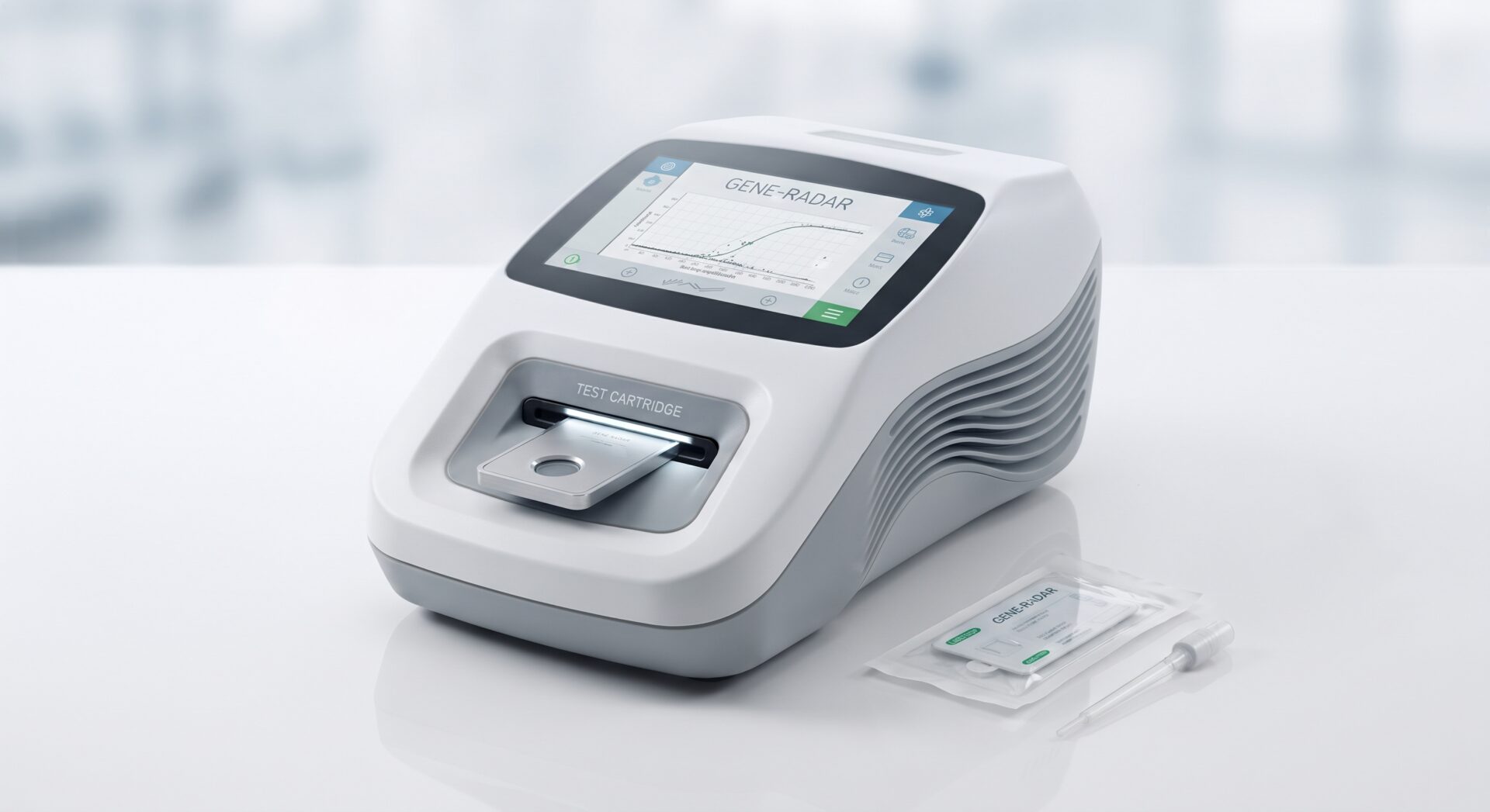
Geek Land USA built a custom i.MX6 quad-core single board computer (SBC) as the core of a purpose-built Medical diagnostic device. The board had to fit an enclosure Geek Land had already designed, drive a 7″ touchscreen, and connect to a companion control board, also designed by Geek Land.
Rather than adapt an off-the-shelf board, Geek Land formalized a custom development program in July 2016. That came after nine months of iterating on the mechanical drawing, from October 2015 to July 2016.

Exploded view of the tablet’s display stack, with adhesive points securing the back of the LCD.
The Challenge
The board had to meet five tight constraints at once.
- Fixed physical envelope. A 150 × 90 mm footprint with 10 mm component height, inside an existing enclosure. Mounting holes needed 6 mm keep-out zones, and extra area was reserved for camera circuitry.
- Full wireless stack on one board. Wi-Fi, Bluetooth, GPS, 3G and a camera, without crowding each other out.
- Hardware security. The USB OTG port could not be exposed through a standard connector anyone could plug into.
- Headless power control. No power button. Power, sleep and reset all had to be driven by signals from an external controller.
- Future-proofing. The hardware had to stay Linux-compatible so the product was not locked into Android.

Mechanical drawing NB-0052 (Rev 6), which fixed the board outline, connector positions and keep-out zones.
The Solution
Geek Land designed an 8-layer board around the i.MX6 Quad with 2 GB DDR3 RAM and 4 GB eMMC flash, running rooted Android 4.4 on a 12–17 V, 3 A input.

Installation illustration: the mainboard mounts behind the display inside Geek Land’s enclosure.
Integrated peripherals
| Function | Component | Design notes |
|---|---|---|
| Display | HE070NA-13C 7″ LCD, 20-pin LVDS FPC | Optional MIPI connector for a 1280×800 panel, removable if space ran out |
| Touch | GKG0366A panel, 6-pin FPC | I²C interface |
| Wi-Fi + Bluetooth | AP6234 combo module | 802.11 b/g/n at 2.4 GHz, Bluetooth 4.0, data only |
| GPS | u-blox MAX-7 | 5 Hz update rate |
| Cellular | Quectel UC15 3G | Data only; SIM socket on the board edge |
| Camera | OV5640 over MIPI | Board-to-FPC connector, 8 cm cable, front-facing |
| Audio | 6-pin Molex | Stereo 8 W speaker out, one mic in |
| Real-time clock | Onboard RTC + CR2032 coin cell | Sized for 2–3 years of backup |
Antennas used IPEX connectors in the prototype so placement could be settled later.
Security by connector choice
The USB OTG interface keeps the standard USB protocol but runs through a 5-pin Molex connector instead of a consumer USB port. It carries data only, for talking to the device’s microcontroller, so an end user cannot plug in a cable and reach the system.
One clean interface to the control board
A single Molex header links the SBC to Geek Land’s sub-board. It carries:
- two USB 2.0 channels
- power-switch and reset inputs
- a sleep-detect output
- a 3.3 V TTL UART at 115200 baud

The Molex header (part 0530471510) that links the SBC to the control board.
Through it, the controller can tell whether the tablet is on, asleep or off. It can also put the tablet to sleep, which turns off the LCD, and shut it down in software. The physical reset switch sits on the sub-board.
Software customizations
The Android build added a custom boot splash screen supplied by Geek Land, brightness control through the standard Settings menu, and root access to the OS.
Engagement Model
Development was scoped at about three months from deposit to working prototypes, with a second board revision planned in from the start.
Scope of work
Geek Land owned the full design: the enclosure, connector layout, sub-board pin definitions, schematic, PCB layout, fabrication and bring-up. Connector positions were signed off after each layout pass.
Schedule
| Phase | Duration |
|---|---|
| Schematic | 10 working days |
| PCB layout | 10 working days |
| PCB fabrication | 3 weeks |
| SMT assembly | 5 working days |
| Software debug | 2 weeks |
| Hardware and software functional test | 2 weeks |
| Second revision, if needed | 3 weeks |
| Final verification | 6 weeks |
Commercial structure
- The R&D fee was split 60% up front and 40% on acceptance of working prototypes, with two prototype sets included.
- Scope changes that forced a board rework were priced and scheduled separately.
- Unit pricing came as a bare mainboard or a fully loaded board with display, camera and radios. The bundle cost about 17% less than buying the modules separately.
- Mainboard unit cost fell about 41% between 10-unit and 1,000-unit quantities.
Lessons Worth Sharing
The biggest lesson: reconcile the mechanical drawing and the contract before layout starts.
Catch spec conflicts early. The drawing (NB-0052, Rev 6) and the agreement disagreed in three places:
- The sub-board header is 16-pin on the drawing but 15-pin in the agreement, with different part numbers.
- The drawing specifies Android 4.0.4 or higher and a 5 V input. The agreement specifies Android 4.4 and 12–17 V.
- The drawing removed the power connector in May 2016, but the agreement still defines a 2-pin power connector.
Finding gaps like these before schematic capture is far cheaper than finding them at the first board spin.
Define scope boundaries explicitly. The agreement states what is out of scope, such as customizing the touch panel after the prototype phase. That clarity heads off disputes later.
Build iteration into the plan. Budgeting a second prototype revision up front made a likely respin a scheduled event rather than a crisis.
Outcome
The project was a successful delivery by Geek Land: working prototypes, then several hundred production units.
- Prototypes delivered. The prototype boards fit the product with only a few modifications.
- Production units shipped. Geek Land produced and delivered several hundred units for production.
- Volume capped by budget. Budget constraints kept volumes from reaching full scale. The hardware itself met its goals.